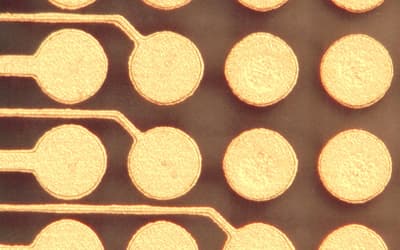
High density interconnect (HDI) structures are being employed in the design of PCBs with dense, high pin-count components and stringent electrical performance requirements. These smaller interconnect geometries benefit complex PCB design in areas such as component and tracking density and overall signal integrity.
HDI layout
The three layout metrics are:
- Layout efficiency: a measure of the amount of traces on an inner layer as a percentage of the maximum that could be on this inner layer.
- Routability predictor: a measure of how easy it is to route the selected traces (at their designated design rules) into the remaining space available.
- Routing density: inches of traces per square inch of inner layer, or cm of traces per sq. cm.
The logical place to start when discussing HDI design is with the IPC guidelines, standards and specifications (www.ipc.org). Four of these specifically apply to HDI design:
- IPC/JPCA-2315, Design Guide for High-density Interconnect Structures and Microvias
- IPC-2226, Sectional Design Standard for High-density Interconnect (HDI) Printed Boards
- IPC/JPCA-4104, Qualification and Performance Specification for Dielectric Materials for High-density Interconnect Structures (HDI)
- IPC-6016, Qualification and Performance Specification for High-density Interconnect (HDI) Structures
The most productive method is to collaborate with the vendor on a stack-up prior to designing the board. That way, the fabricator will be able to make minimal adjustments to meet your goals. We support HDI technologies and we have used laser processing for microvia (blind / buried / plugged) formation for a number of years with great success.
Via / hole sizes
| Min. hole size drilled | Min. hole size plated | Aspect ratio | |
|---|---|---|---|
| PTH | 0.15 mm | 0.1 mm | 1:25 |
| Buried via / hole | 0.1 mm | – | 1:25 |
| Blind via | 0.1 mm | 0.05 mm | 1:1 |
| Laser via | 0.075 mm | 0.025 mm | – |
| Depth drilling | ±10 µm | – | – |
- Standard drilled hole to copper feature: min. 0.2 mm
- Drill position tolerance: ±0.35 mm
If you are interested in a professional European PCB supplier, please feel free to call me under +49 162 2609836 or send me your request directly to the following email address: kao@pcbexpress.eu